 After many rumors and suppositions, AMD has finally unveiled the approximate retail price of their upcoming high-performance eight-core FX-Series processors. Just as expected, these will cost around $300, which is about the same as the pricing set by Intel for its Sandy Bridge flagship, the Core i7-2600K.
“Top tier prizes: Five (5) AMD FX series eight-core processors. Approximate Retail Value: $300 USD each,” reads the competition's official rules.In comparison, Intel's fastest desktop processor based on the Sandy Bridge architecture, the Core i7-2600K, also retails for just a bit over $300, which seems to suggest that performance should be about equal.From what we do know at this point in time, the FX-8150P should be AMD's most powerful FX-series chip as it features four Bulldozerprocessor modules for a total of eight computing cores, 8MB of Level 2 cache as well as 8MB of Level 3 cache.The chip will sport a base frequency of 3.6GHz, which can be increased up to 4.2GHz thanks to the Turbo Core technology, and its TDP is set at 125W.AMD plans to launch this processor together with three other chips, including another eight-core model that is known as the FX-8100, which packs similar specifications with the FX-8150P.However, the FX-8100 will feature lower clock speeds, 2.8GHz base and 3.7GHz maximum Turbo, to allow AMD to drop its TDP to 95W.The two other AMD Bulldozer CPUs expected to launch are the FX-6100 and FX-4100, which sport six and four processing cores, respectively.Both of these include 8MB of L3 cache as their older siblings, but feature less L2 cache and lower clock speeds. No information regarding the pricing of the six and quad-core processors is available at this point in time. The release date is also unknown, but most rumors place it in September or October of 2011.
Semua informasi tersebut ditemukan pada sebuah forum Cina, yang juga memberikan serangkaian hasil benchmark untuk menunjukkan kinerja chip.
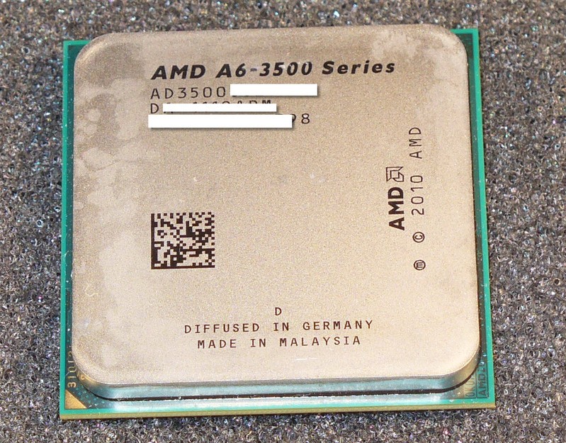
AMD baru APU akan disebut A6-3500 dan spesifikasi yang mirip dengan yang dari-A6 3600, kecuali untuk inti komputasi keempat yang telah dinonaktifkan oleh AMD.
Ini berarti bahwa chip memiliki frekuensi dasar 2.1GHz, yang bisa naik berkat teknologi 2.4GHz core AMD Turbo, 3MB Level 2 cache memory, dan terpadu GPU Radeon HD 6530D.
Paling lambat kedua core grafis yang terintegrasi dalam lineup Llano, yang mencakup 6530D HD 320 stream processor clock 433MHz, dan kompatibel dengan teknologi Hybrid CrossFireX perusahaan untuk memungkinkan dual-grafis operasi.
Luar dari inti grafis on-die, baru Llano APU juga akan menampilkan dual-channel DDR3-1866MHz terintegrasi kontroler memori dan sebuah 16-lane PCI Express Gen 2.0 kontroler, sedangkan TDP dinilai pada 65W yang sama seperti yang dari A6-3600.
AMD A6-3500 tiga core AMD Llano APU - Benchmark skor dan spesifikasi
Dalam rangka untuk menguji kinerja dari chip tri-core Llano, pengguna menjalankan kedua 3DMark 06 dan cache & patokan memori dari software suite AIDA64. Pada bagian pertama dari dua skenario, A6-3500 berhasil mencapai skor 3D mark 5173.
Sayangnya, pengguna tidak mencoba untuk membuka inti cacat keempat, jadi kita tidak tahu apakah chip ini dapat berubah menjadi bagian quad-core murah.
AMD baru A6-3500 triple-core APU diharapkan tiba pada kuartal ketiga tahun ini pada titik harga yang belum diungkapkan.

A few days ago, we reported that AMD is preparing to launch triple-core version of the Llano accelerated processing unit, and today, after a little digging around, we managed to find the first pictures of the APU and screenshot series, which confirms the specifications.
All information is found on a Chinese forum, which also provides a series of benchmark results to demonstrate the performance of the chip.
The new AMD APU will be called A6-3500 and similar specifications to that of the A6-3600, except for the four computational core that has been disabled by AMD.
This means that the chip has a fundamental frequency of 2.1GHz, which could rise thanks to the technological core AMD Turbo 2.4GHz, 3MB Level 2 cache memory, and integrated GPU Radeon HD 6530D.
Second slowest integrated graphics core in Llano lineup, which includes HD 6530D 433MHz clock 320 stream processors, and compatible with Hybrid CrossFireX technology companies to enable dual-graphics operations.
Outside of the graphics core on-die, New Llano APU will also feature dual-channel DDR3-1866MHz integrated memory controller and a 16-lane PCI Express Gen 2.0 controller, while the TDP is rated at 65W the same as that of the A6-3600.
A6-3500 AMD three core AMD Llano APU - Benchmark scores and specifications
In order to test the performance of the tri-core chips Llano, users run both 3DMark 06 and cache & memory benchmark suite of software AIDA64. In the first of the two scenarios, A6-3500 managed to reach the 3D mark score of 5173.
Unfortunately, users do not try to open a fourth core disabled, so we do not know if this chip can be turned into a cheap quad-core parts.
A6-3500 new AMD triple-core APU is expected to arrive in the third quarter of this year at a price point that has not been disclosed.
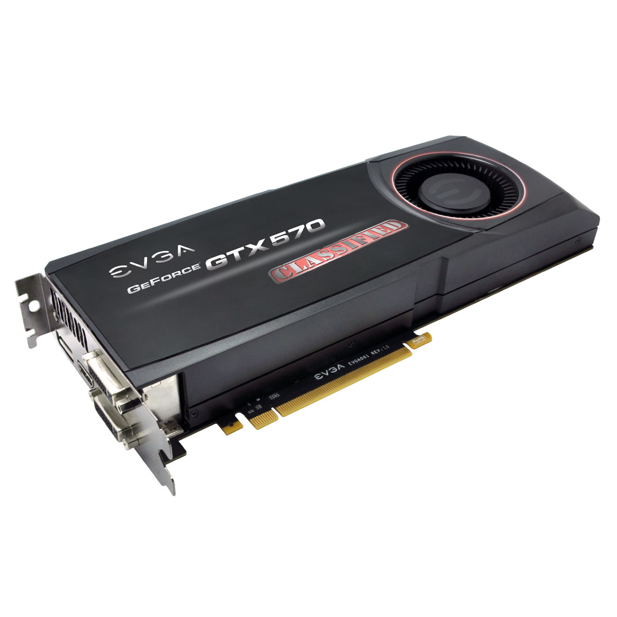
Mengambil melihat pada penciptaan EVGA terbaru, menjadi jelas bahwa solusi pendingin yang digunakan sangat mirip dengan desain referensi Nvidia.
Namun, ini telah tweak untuk mengatasi peningkatan jumlah panas yang dihasilkan oleh overclocking dan EVGA bahkan didesain ulang papan sirkuit cetak kartu.
Dibandingkan dengan PCB standar, ini sekarang memiliki desain 10-lapisan, sebuah 6-fase digital canggih GPU VRM, yang EVGA menyatakan bahwa overclocking headroom dapat meningkatkan, serta titik tegangan berdedikasi pembacaan.
Modifikasi tambahan juga dibawa ke sistem tenaga pengiriman, sebagai kartu sekarang membawa 6 dan 8-pin PCI-Express konektor power, yang dapat memberikan hingga 225W daya (slot PCI Express menyediakan 75W tambahan).
Semua perubahan ini memungkinkan EVGA untuk meningkatkan jam operasi dari GeForce GTX 570 untuk 822MHz Baris untuk GPU dan 975MHz (3.9GHz efektif) untuk memori.
Untuk meletakkan segala sesuatu ke dalam perspektif, versi saham dari 570 GTX memiliki inti berjalan di 732MHz, sedangkan memori bekerja pada 950MHz (3800MHz data rate).
Kartu EVGA juga termasuk berukuran penuh konektor HDMI 1,4 serta output DisplayPort, di samping pasangan biasa dual-link DVI konektor.
Nvidia GeForce GTX 570 didasarkan pada GPU GF110 perusahaan dan paket stream prosesor 480, 60 texture unit, 40 ROP unit dan bus memori 320-bit lebar yang terhubung ke 1.25GB GDDR5 video buffer.
Harga untuk GeForce GTX 570 Baris telah dibentuk di $ 359,99, tapi kartu ini belum tersedia dalam stok. On the first day of Computex, EVGA has announced that the company is working on delivering the line version of the popular card Nvidia GeForce GTX 570 graphics, and now, about a month after the fair closed its gates, the card company was finally registered on the site.
Taking a look at EVGA latest creation, it became clear that the cooling solution used is very similar to Nvidia's reference design.
However, this has been tweaked to handle the increased amount of heat generated by overclocking and EVGA even redesigned printed circuit board card.
Compared with standard PCB, it now has a 10-layer design, an advanced 6-phase digital VRM GPU, the EVGA state that can increase overclocking headroom, as well as dedicated point voltage readings.
Additional modifications are also taken to the power delivery system, as the cards now carry 6 and 8-pin PCI-Express power connectors, which can provide up to 225W power (PCI Express slot provides additional 75W).
All these changes allow EVGA to increase hours of operation of the GeForce GTX 570 to 822MHz for the GPU and 975MHz Lines (3.9GHz effective) for the memory.
To put things into perspective, the stock version of the GTX 570 has a core running at 732MHz, while the memory works at 950MHz (3800MHz data rate).
Card EVGA also includes full-sized HDMI 1.4 and DisplayPort output, in addition to ordinary pair of dual-link DVI connectors.
Nvidia GeForce GTX 570 GPU is based on the company and package GF110 480 stream processors, 60 texture units, 40 ROP units and 320-bit memory bus width which is connected to 1.25GB GDDR5 video buffer.
Prices for the GeForce GTX 570 line has been established at $ 359.99, but this card is not available in stock.
Menurut OCWorkbench, meskipun unit pengolahan AMD A8-3850 dipercepat muncul untuk olahraga multiplier unlocked, ini tidak benar-benar terjadi karena setelan ini di atas nilai default 29x tidak membawa perbaikan dalam kinerja.
Akibatnya, kecepatan clock tinggi yang dilaporkan oleh kedua CPU-Z dan BIOS sebenarnya keliru dan chip masih beroperasi pada 2.9GHz, bahkan jika beberapa alat pengembalian yang lebih tinggi daripada frekuensi saham.
Sekarang, kita tidak tahu apakah kesalahan disebabkan oleh semacam kesalahan BIOS motherboard atau jika beberapa isu lain yang harus disalahkan.
Unit pengolahan A8-3850 dipercepat diperkenalkan pada tanggal 30 Juni dan paling kuat Fusion AMD chip untuk saat ini.
APU paket core pemrosesan empat, yang beroperasi pada 2.9GHz, 4MB Level 2 cache, dan Radeon HD 6550D unit grafis.
Ini mencakup tidak kurang dari 400 unit shader clock di 600MHz dan dapat bekerja sama dengan memilih kartu grafis diskrit dalam mode CrossFireX Hibrida.
Luar dari inti grafis on-die, chip Llano juga fitur controller memori dual-channel DDR3 1866MHz terintegrasi-dan 16-lane PCI Express Gen 2.0 kontroler.
Unit pengolahan dipercepat yang kompatibel dengan motherboard soket FM1. Ini dapat didukung oleh chipset A55 atau A75, dan menawarkan fitur keduanya mirip, kecuali untuk USB 3.0 dan SATA 6Gbps dukungan, yang hanya ditemukan di FCH A75 lebih maju.
AMD A8-3850 APU benar tersedia sebagai kita berbicara dari berbagai pengecer di seluruh dunia dan di Amerika Serikat ini dijual seharga sekitar $ 139,99. In the short time that AMD desktop Llano APUs have been out on the market, a series of CPU-Z screenshots have revealed this chip reaches far above the frequency of 5GHz, but the real surprise it seems that, while these reports seem legit, the APUs are not really working lowing the clock speeds.
According OCWorkbench, although the processing unit A8-3850 AMD accelerated appears to sport an unlocked multiplier, it does not really happen because the setting is above the default value of 29x does not bring improvement in performance.
As a result, the high clock speed reported by CPU-Z and the second BIOS chip is actually wrong and still operate at 2.9GHz, even if some of the tools a higher return than the stock frequency.
Now, we do not know whether such errors are caused by the motherboard BIOS error or if some other issues are to blame.
Unit A8-3850 accelerated processing was introduced on June 30 and most powerful AMD Fusion chip to date.
APU package of four processing cores, which operates at 2.9GHz, 4MB Level 2 cache, and the Radeon HD graphics unit 6550D.
This includes no less than 400 shader units clocked at 600MHz and can work together to choose a discrete graphics cards in CrossFireX mode hybrid.
Outside of the graphics core on-die, chip Llano also features dual-channel memory controller integrated DDR3 1866MHz-and 16-lane PCI Express Gen 2.0 controller.
Accelerated processing unit that is compatible with the motherboard socket FM1. This can be supported by the chipset A55 or A75, and offers features both similar, except for USB 3.0 and SATA 6Gbps support, which is found only in more advanced FCH A75.
AMD A8-3850 APU is available as we speak from various retailers around the world and in the United States is sold for around $ 139.99.