
Semua informasi tersebut ditemukan pada sebuah forum Cina, yang juga memberikan serangkaian hasil benchmark untuk menunjukkan kinerja chip.
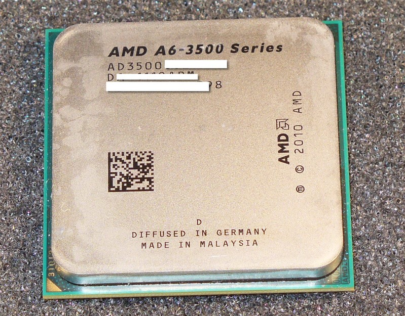
AMD baru APU akan disebut A6-3500 dan spesifikasi yang mirip dengan yang dari-A6 3600, kecuali untuk inti komputasi keempat yang telah dinonaktifkan oleh AMD.
Ini berarti bahwa chip memiliki frekuensi dasar 2.1GHz, yang bisa naik berkat teknologi 2.4GHz core AMD Turbo, 3MB Level 2 cache memory, dan terpadu GPU Radeon HD 6530D.
Paling lambat kedua core grafis yang terintegrasi dalam lineup Llano, yang mencakup 6530D HD 320 stream processor clock 433MHz, dan kompatibel dengan teknologi Hybrid CrossFireX perusahaan untuk memungkinkan dual-grafis operasi.
Luar dari inti grafis on-die, baru Llano APU juga akan menampilkan dual-channel DDR3-1866MHz terintegrasi kontroler memori dan sebuah 16-lane PCI Express Gen 2.0 kontroler, sedangkan TDP dinilai pada 65W yang sama seperti yang dari A6-3600.
AMD A6-3500 tiga core AMD Llano APU - Benchmark skor dan spesifikasi
Dalam rangka untuk menguji kinerja dari chip tri-core Llano, pengguna menjalankan kedua 3DMark 06 dan cache & patokan memori dari software suite AIDA64. Pada bagian pertama dari dua skenario, A6-3500 berhasil mencapai skor 3D mark 5173.
Sayangnya, pengguna tidak mencoba untuk membuka inti cacat keempat, jadi kita tidak tahu apakah chip ini dapat berubah menjadi bagian quad-core murah.
AMD baru A6-3500 triple-core APU diharapkan tiba pada kuartal ketiga tahun ini pada titik harga yang belum diungkapkan.

A few days ago, we reported that AMD is preparing to launch triple-core version of the Llano accelerated processing unit, and today, after a little digging around, we managed to find the first pictures of the APU and screenshot series, which confirms the specifications.
All information is found on a Chinese forum, which also provides a series of benchmark results to demonstrate the performance of the chip.
The new AMD APU will be called A6-3500 and similar specifications to that of the A6-3600, except for the four computational core that has been disabled by AMD.
This means that the chip has a fundamental frequency of 2.1GHz, which could rise thanks to the technological core AMD Turbo 2.4GHz, 3MB Level 2 cache memory, and integrated GPU Radeon HD 6530D.
Second slowest integrated graphics core in Llano lineup, which includes HD 6530D 433MHz clock 320 stream processors, and compatible with Hybrid CrossFireX technology companies to enable dual-graphics operations.
Outside of the graphics core on-die, New Llano APU will also feature dual-channel DDR3-1866MHz integrated memory controller and a 16-lane PCI Express Gen 2.0 controller, while the TDP is rated at 65W the same as that of the A6-3600.
A6-3500 AMD three core AMD Llano APU - Benchmark scores and specifications
In order to test the performance of the tri-core chips Llano, users run both 3DMark 06 and cache & memory benchmark suite of software AIDA64. In the first of the two scenarios, A6-3500 managed to reach the 3D mark score of 5173.
Unfortunately, users do not try to open a fourth core disabled, so we do not know if this chip can be turned into a cheap quad-core parts.
A6-3500 new AMD triple-core APU is expected to arrive in the third quarter of this year at a price point that has not been disclosed.