
Pada hari pertama Computex, EVGA telah mengumumkan bahwa perusahaan bekerja pada memberikan versi Baris kartu populer Nvidia GeForce GTX 570 grafis, dan sekarang, sekitar sebulan setelah adil ditutup gerbangnya, kartu itu akhirnya terdaftar di perusahaan situs.
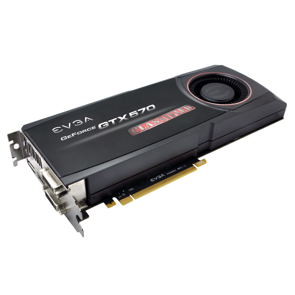
Mengambil melihat pada penciptaan EVGA terbaru, menjadi jelas bahwa solusi pendingin yang digunakan sangat mirip dengan desain referensi Nvidia.
Namun, ini telah tweak untuk mengatasi peningkatan jumlah panas yang dihasilkan oleh overclocking dan EVGA bahkan didesain ulang papan sirkuit cetak kartu.
Dibandingkan dengan PCB standar, ini sekarang memiliki desain 10-lapisan, sebuah 6-fase digital canggih GPU VRM, yang EVGA menyatakan bahwa overclocking headroom dapat meningkatkan, serta titik tegangan berdedikasi pembacaan.
Modifikasi tambahan juga dibawa ke sistem tenaga pengiriman, sebagai kartu sekarang membawa 6 dan 8-pin PCI-Express konektor power, yang dapat memberikan hingga 225W daya (slot PCI Express menyediakan 75W tambahan).
Semua perubahan ini memungkinkan EVGA untuk meningkatkan jam operasi dari GeForce GTX 570 untuk 822MHz Baris untuk GPU dan 975MHz (3.9GHz efektif) untuk memori.
Untuk meletakkan segala sesuatu ke dalam perspektif, versi saham dari 570 GTX memiliki inti berjalan di 732MHz, sedangkan memori bekerja pada 950MHz (3800MHz data rate).
Kartu EVGA juga termasuk berukuran penuh konektor HDMI 1,4 serta output DisplayPort, di samping pasangan biasa dual-link DVI konektor.
Nvidia GeForce GTX 570 didasarkan pada GPU GF110 perusahaan dan paket stream prosesor 480, 60 texture unit, 40 ROP unit dan bus memori 320-bit lebar yang terhubung ke 1.25GB GDDR5 video buffer.
Harga untuk GeForce GTX 570 Baris telah dibentuk di $ 359,99, tapi kartu ini belum tersedia dalam stok.
On the first day of Computex, EVGA has announced that the company is working on delivering the line version of the popular card Nvidia GeForce GTX 570 graphics, and now, about a month after the fair closed its gates, the card company was finally registered on the site.
Taking a look at EVGA latest creation, it became clear that the cooling solution used is very similar to Nvidia's reference design.
However, this has been tweaked to handle the increased amount of heat generated by overclocking and EVGA even redesigned printed circuit board card.
Compared with standard PCB, it now has a 10-layer design, an advanced 6-phase digital VRM GPU, the EVGA state that can increase overclocking headroom, as well as dedicated point voltage readings.
Additional modifications are also taken to the power delivery system, as the cards now carry 6 and 8-pin PCI-Express power connectors, which can provide up to 225W power (PCI Express slot provides additional 75W).
All these changes allow EVGA to increase hours of operation of the GeForce GTX 570 to 822MHz for the GPU and 975MHz Lines (3.9GHz effective) for the memory.
To put things into perspective, the stock version of the GTX 570 has a core running at 732MHz, while the memory works at 950MHz (3800MHz data rate).
Card EVGA also includes full-sized HDMI 1.4 and DisplayPort output, in addition to ordinary pair of dual-link DVI connectors.
Nvidia GeForce GTX 570 GPU is based on the company and package GF110 480 stream processors, 60 texture units, 40 ROP units and 320-bit memory bus width which is connected to 1.25GB GDDR5 video buffer.
Prices for the GeForce GTX 570 line has been established at $ 359.99, but this card is not available in stock.